NTNU NanoLab · Thesis project
Artificial spin ice on glass
Fabricating magnetic pinwheel arrays on transparent glass, toward studying two coupled magnetic layers with light.
Tiny magnets, imaged from behind
While artificial intelligence and neural networks see expanding societal adoption, the underlying hardware supporting these workloads is approaching the fundamental limits of conventional scaling. The Von Neumann architecture separates memory and processing into distinct units, and data movement between them affects the runtime and energy cost in neural network workloads. Neuromorphic computing offers an alternative method by performing computation and memory access in the same physical stack. Rather than emulating neural behavior in software on standard silicon, this approach exploits the intrinsic dynamics of physical systems to process and store information at the same time.
Artificial spin ice (ASI) is one such physical system. ASI consists of patterned ferromagnetic nanoislands arranged in a lattice, where each island acts as a binary element whose moment points along one of two directions set by shape anisotropy. The collective state of the array is governed by the dipolar interactions between islands and can be tuned through the lattice geometry and island dimensions. ASI provides a platform for studying frustrated magnetism in a system where the elements are individually accessible, and the same degree of magnetic control opens the door for logic circuits and physical neuromorphic networks. In the specialization project and current master thesis I am working on fabricating and characterizing ASI hybrid devices on an optically transparent substrate.
Fabricating ASI hybrid devices on glass
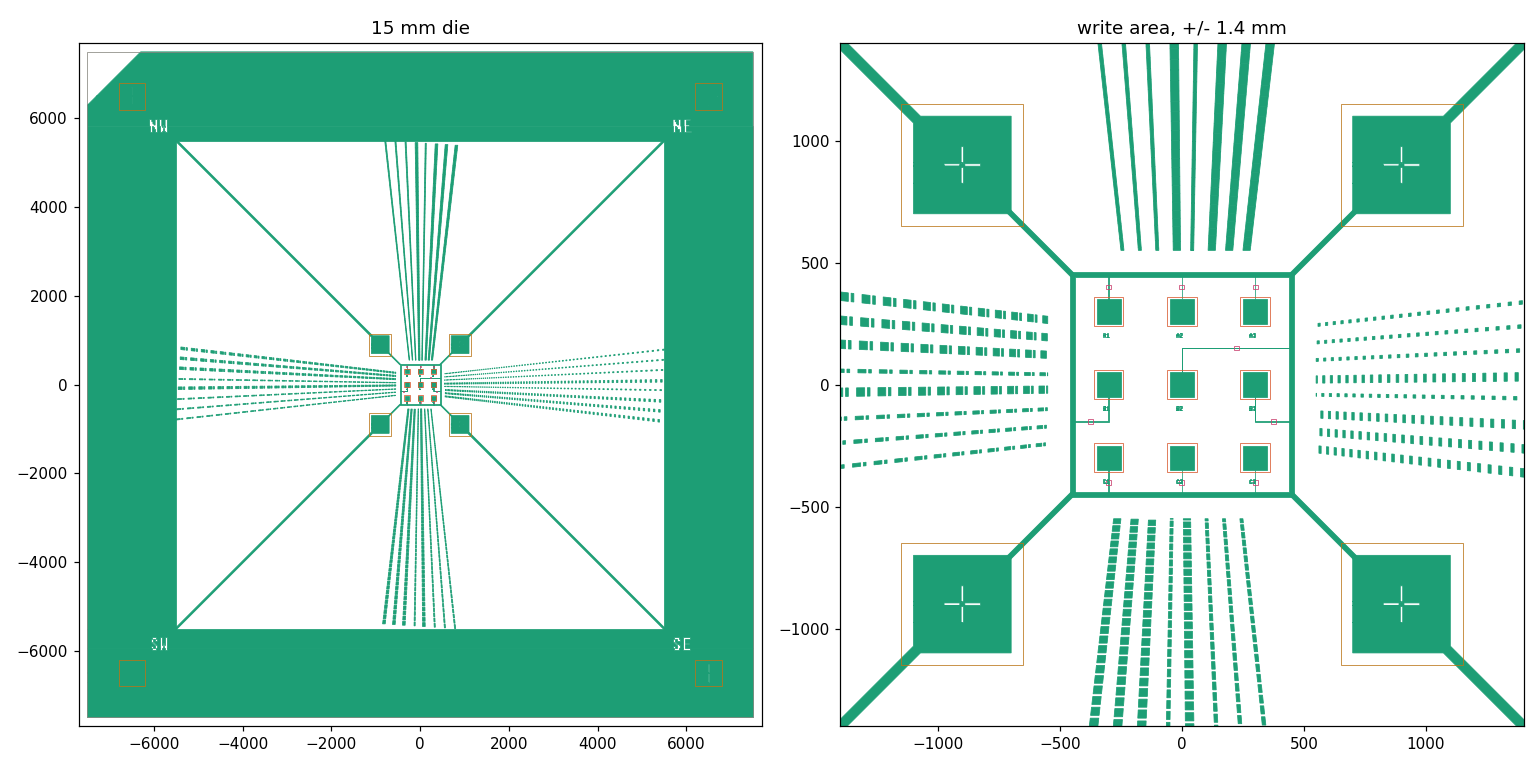
The specialization project established a fabrication route for ASI hybrid devices with a bilayer architecture. A Ni80Fe20 (Permalloy) pad, defined by photolithography, served as the underlayer for the ASI nanoislands patterned by electron beam lithography (EBL). Both layers were deposited by electron-beam evaporation and patterned using lift-off.
The optical transparency of the glass substrate enables a flip-chip backside magneto-optical Kerr effect (MOKE) geometry for depth-selective magnetic characterization and imaging. The fabrication work examined EBL dose and Permalloy thickness to establish a process window, and assessed the effect of an Electra 94 conductive coating on charging at the insulating substrate.
Charging, resist thickness and pattern definition
Samples exposed with the Electra 94 coating showed substantially improved pattern definition compared with uncoated samples, consistent with in situ observations of charging during EBL. At a fixed dose factor of 1.4 (approximately 168 µC/cm2), SEM imaging also showed a strong dependence on Permalloy underlayer thickness: the 20 nm underlayer produced well-defined islands, while the 10 nm underlayer gave visibly degraded geometry.
Spectral reflectometry identified the CSAR 62 resist film used in the first fabrication run as approximately 750 nm thick, against an intended thickness of 95 nm. A subsequent run using custom-diluted resist produced a defined pinwheel array on a 20 nm Permalloy underlayer at dose factor 1.4, with the sublattice arrangement recognizable across the imaged cell.
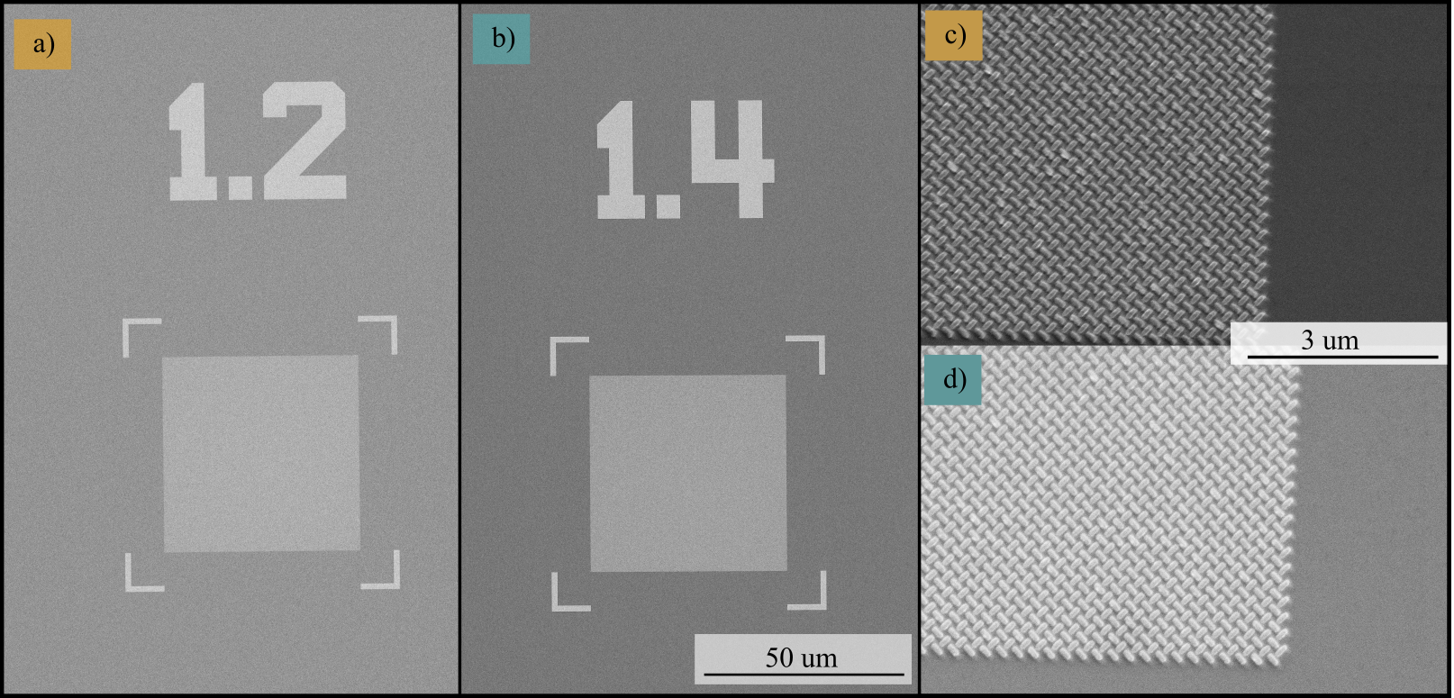
Beam-driven charging limited high-magnification SEM imaging beyond 25,000×, so island dimensions on the final samples were not extracted. The dose conclusion is therefore restricted to a clearing dose above factor 1.2, with both fabrication rounds indicating factor 1.4 or higher as a viable working point. These results establish a basis for further process refinement rather than a precisely determined optimum dose.
Magnetic characterization
MOKE microscopy of the 20 nm device showed magnetic contrast between the patterned array and the surrounding film, confirming a measurable magnetic signal from the ASI region. This demonstrated magnetic contrast in the fabricated device; full hysteretic separation of the island and underlayer contributions in the backside geometry remained for subsequent work.
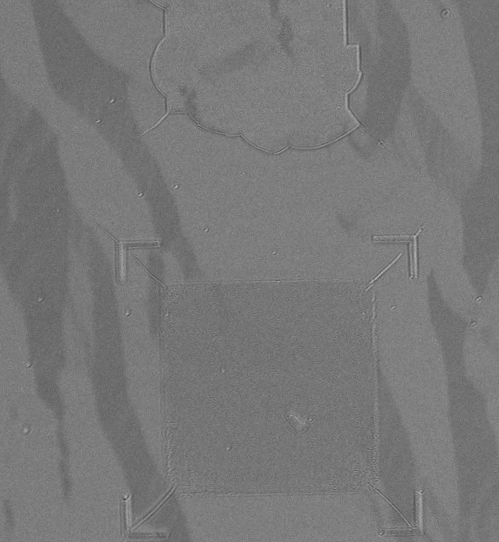
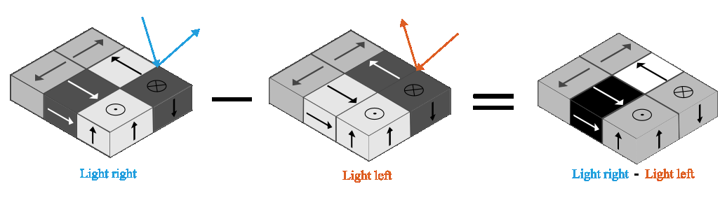
MOKE microscopy detects magnetization-dependent changes in the polarization of reflected light. With opposing illumination directions, the longitudinal magnetic contrast reverses. Subtracting the two images helps suppress the shared nonmagnetic optical contrast and isolate the magnetic contribution.
From specialization project to master’s thesis
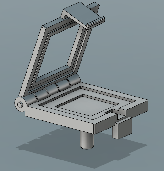
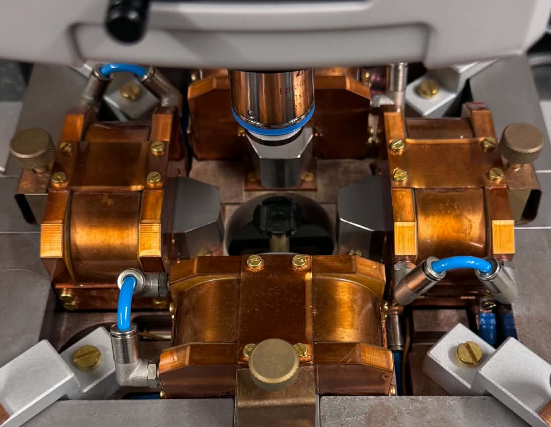
A custom 3D-printed sample holder was prepared for the flip-chip backside imaging geometry. The specialization project established the fabrication route and demonstrated magnetic contrast, while leaving separation of the island and underlayer hysteresis responses to the continuing master’s work.
The current work builds on this foundation through a revised underlayer mask and sample-holder design for backside optical access. Further steps include refining the exposure dose, reducing charging sufficiently to measure island dimensions reliably, and addressing the optical back-reflection that limited high-magnification backside imaging.